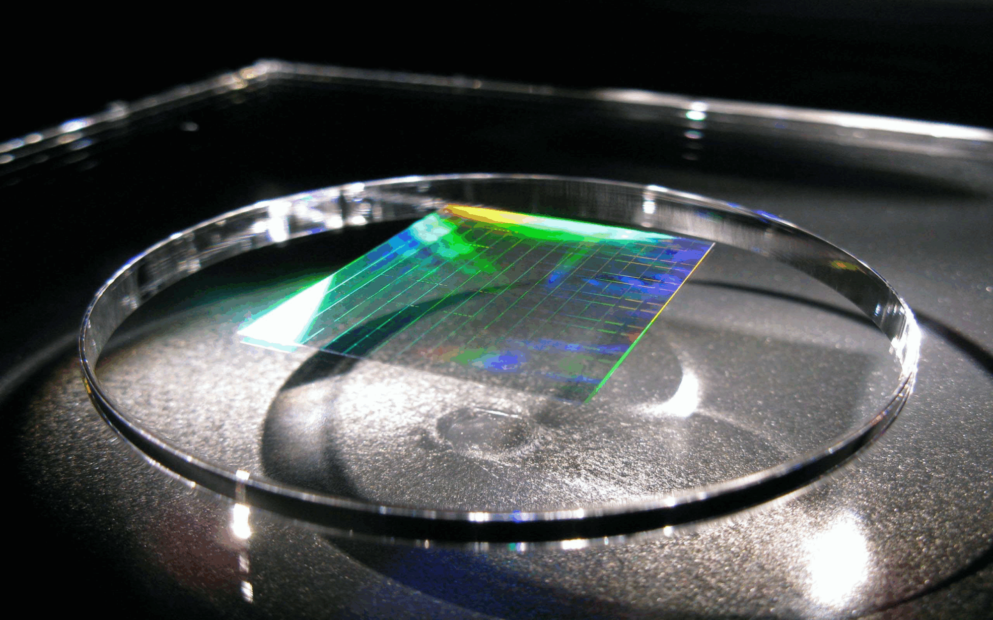
Canon Nanotechnologies has developed a comprehensive suite of technologies that enable precise and scalable UV nanoimprint lithography (UV-NIL) for advanced semiconductor manufacturing. At the core of this technology is step-and-flash imprint lithography (S-FIL®), a UV-curable process that patterns sub-10nm features by physically molding resist material between a transparent template and a wafer surface. This technique enables exceptional resolution and pattern fidelity without the need for complex optics or multi-patterning, making it a compelling solution for advanced nodes. Canon’s proprietary nanoimprint systems are built for full-field patterning on 300mm wafers, delivering production-level throughput while maintaining tight overlay and critical dimension control.
To support this precision, Canon Nanotechnologies has developed advanced nanopositioning hardware capable of nanometer alignment accuracy between the wafer and template, a critical requirement for overlay-sensitive semiconductor applications. In parallel, the company has engineered shape control systems that actively manage distortions in both wafers and masks to ensure uniform contact and pattern transfer across the entire substrate. Canon’s high-performance dispensing technology delivers sub-picoliter drops of imprint resist with precise placement, enabling uniform pattern fill with minimal material usage. Additionally, ongoing innovations in defect reduction—including particle control, template cleaning, and resist filtration—ensure the reliability and yield performance required for high-volume manufacturing. These integrated technologies collectively position Canon Nanotechnologies at the forefront of scalable, next-generation lithography solutions.